Breakthrough in 2D flash chip achieved
In a world first, integrated technology can speed up AI computing system


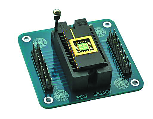
A research team from Shanghai-based Fudan University has developed the world's first full-featured, 2D flash chip enabled by system integration, marking a milestone in the engineering of 2D electronic devices.
This breakthrough integrates the ultrafast 2D flash memory device with a mature silicon-based complementary metal oxide semiconductor, or CMOS technology, providing a model to accelerate the transition of next-generation disruptive devices from research to application and offering strong support for advancing information technology to a new high-speed era.
The chip supports eight-bit instruction operations, 32-bit high-speed parallel operations and random access, achieving a memory cell yield of 94.3 percent. Its operation speed surpasses current flash memory technology, marking the first engineering realization of a 2D-silicon hybrid flash chip, the scientists said.
On Wednesday, a paper detailing the research results was published in the journal Nature.
In the era of artificial intelligence, the demands for faster data access have grown dramatically, while the limited speed and power consumption of traditional memory technologies have become bottlenecks in the AI computing system.
In April, the same team introduced the PoX 2D flash memory prototype in Nature, achieving an unprecedented program speed of 400 picoseconds, the fastest semiconductor charge storage technology to date.
However, the process of industrializing disruptive innovations for system-level applications often takes a prolonged time. The team from Fudan University's State Key Laboratory of Integrated Chips and Systems as well as College of Integrated Circuits and Micro-nano Electronics strategically integrated their 2D flash technology into the industry's CMOS platform, providing a way to turn the concept of the 2D electronics device into a complex system application.
"It took about 24 years from the first prototype semiconductor transistor to the first CPU. However, by integrating emerging technologies into the existing CMOS platform, the process in our research is significantly compressed. We can further accelerate the exploration of disruptive applications in the future," said Liu Chunsen, a first author and also corresponding author of the paper.
Zhou Peng, another corresponding author of the paper and a lead researcher on the team, said that they believed storage devices are likely to be the first type of 2D electronic devices to be industrialized due to their modest demands on material quality and manufacturing processes, coupled with performance metrics that far exceed current technologies.
Scientists explained that the chips that people talk about today are mostly made from silicon. Silicon materials and 2D materials are vastly different, as silicon wafers are typically hundreds of micrometers thick, while 2D semiconductor materials are at the atomic thickness level, equivalent to a thickness of less than 1 nanometer.
A core challenge for the team was how to integrate the 2D materials with CMOS technology without compromising performance. The surface of a CMOS circuit is quite rough due to the underlying components, while the 2D semiconductor materials are only 1 to 3 atoms thick. Such materials can easily break if they are directly placed on CMOS circuits.
"This is like looking at Shanghai from space. It seems flat, but within the city, there are buildings of varying heights — over 400 meters, 100 meters, or just a few dozen meters. If you lay a thin film over the city, the film itself would not be flat," said Zhou, adding that this explains why researchers worldwide in 2D semiconductors can only process materials on extremely flat native substrates so far.
In their research, the team decided to start with 2D materials that inherently possess a certain degree of flexibility. By employing a modular integration approach, the scientists fabricated the 2D memory circuits on the mature CMOS circuits and used high-density monolithic interconnection technology for communication between different modules. This innovative core process allows for the tight coupling of 2D materials with CMOS substrates at the atomic scale.
The research team said that the newly developed chip has successfully completed the tape-out process. For the next step, the researchers plan to set up a pilot production line and collaborate with relevant institutions to establish an engineering project, aiming to integrate it to a megabyte-level scale within the next three to five years.
Experts noted that the current bottleneck for AI systems is shifting from front-end computing power to back-end storage and data, and future models will become increasingly large. Some industry experts expressed optimism that this achievement will transition from lab to large-scale applications at a faster pace, integrating into scenarios such as personal computers and mobile devices.
"This research represents a 'source technology' in China's integrated circuit field, allowing the country to take the lead in nextgeneration core storage technologies," said Zhou.
zhouwenting@chinadaily.com.cn


- Former Hainan official sentenced in bribery case
- Hangzhou residents enjoy rare snowfall
- Artificial reefs part of successful marine conservation efforts in Guangdong
- Zigong lantern festival combines cultural heritage with advanced technology
- Woman executed for abusing and killing stepdaughter
- Zhangjiakou academy students hit Olympic ski slopes as winter break begins