New machine raises country's image in photolithography


"Make it small" has been the mantra that drives big developments in microelectronics, from transistors to processors. So much so that high-tech companies' competitiveness rests on the ability to reliably create components on the scale of nanometers, or one-billionth of a meter.
At the heart of microengineering lies photolithography, one of the key techniques used to create the circuitry patterns on semiconductor chips. This allows engineers to pack and replicate complicated circuits with millions of components into a very tiny space using light.
This technique is so advanced that only a handful of companies from Europe and Japan can produce the machine capable of such a feat. But recently, China entered the game.
The Institute of Optics and Electronics under the Chinese Academy of Sciences announced on Thursday that it has developed its own photolithography machine, thus overcoming one of the major engineering obstacles limiting China's development in chips, nanocomponents and optical instruments.
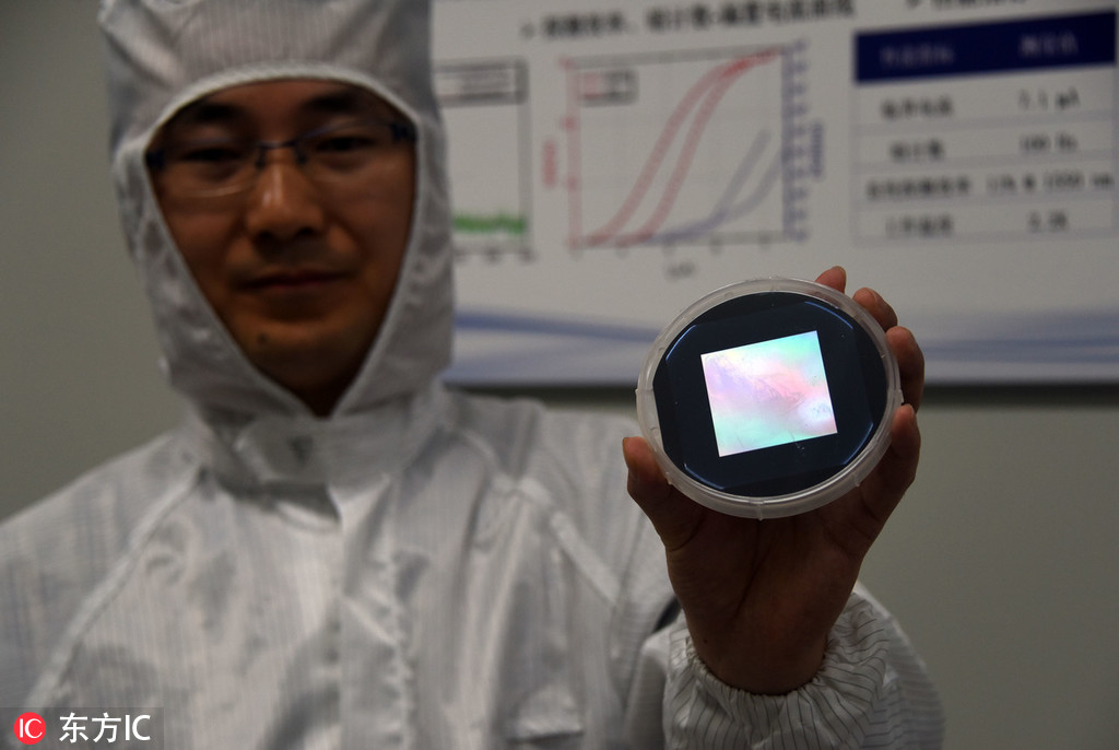
The new machine, which scientists began building in 2012, can etch circuitry patterns less than 22 nanometers using ultraviolet light. Combined with other techniques, it can be used in the future to create chips of around 10 nanometers.
"The machine is of great value in manufacturing general chips and other materials that require microengineering, including some integrated circuits," said Hu Song, deputy chief designer of the project.
The machine can also be used to make small components for applications such as sensors, detectors and biochips, Hu said.
It is already being used by several institutions including Sichuan University and the University of Electronic Science and Technology of China.
However, the new machine's production capability is still small, hence it is still limited to producing key components for research, Hu said.
In the coming years, the teamwill focus its efforts on increasing the machine's productivity to industrial scale. There are still substantial gaps in the microengineering sector between China and developed countries, but China is catching up fast, Hu said.
Companies capable of photolithography will have an overwhelming edge in producing microelectronics, he said. Chip manufacturing giant Intel claimed it could produce more than 5 billion nanoscale transistors every second, according to its company's fact sheet.
The world's largest photolithography supplier is a Dutch company called ASML Holding. Some of ASML's main competitors are Canon and Nikon.
Since the late 1990s, China has been blocked from importing cutting-edge photolithography technologies and other chip manufacturing equipment from developed countries.
This situation is aggravated because ASML owns substantial patents covering imprint lithography, which includes photolithography, Hu said.
As a result, Chinese companies have to rely on relatively outdated and inefficient techniques to produce microelectronics, thus their product is often inferior to that of developed countries.
To overcome the monopoly, the Institute of Optics and Electronics discovered a new physics phenomenon in 2003 and used the property as the basis for the new machine.
China now has 47 domestic and four international patents regarding the new technology, Hu said.
"We no longer fear a foreign technical blockade because we have full intellectual ownership of the new technique."


- China expects over 2.05 million daily cross-border trips during Spring Festival holiday
- Xinjiang through my eyes: Maierdan's cafe of memory
- Chinese researchers build quantum key distribution chip network covering 3,700 km
- Hong Kong sectors voice strong support for Jimmy Lai's sentence
- Mainland official extends greetings to Taiwan compatriots ahead of Chinese New Year
- Legislator highlights AI, tech and awareness to reduce weather risks